TSV interposer

Advanced TSV Packaging Solutions
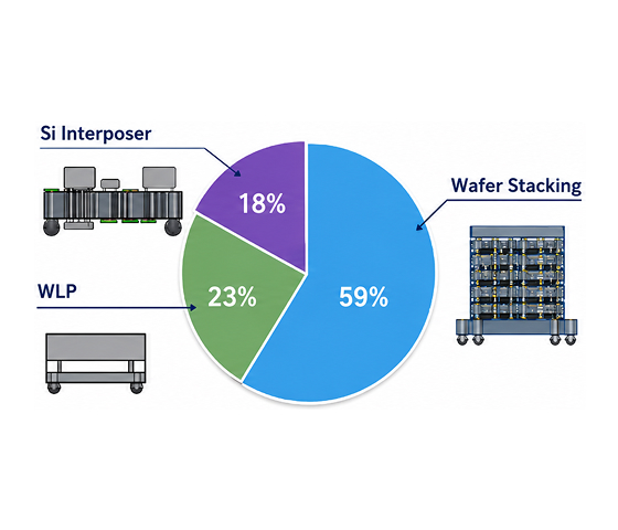
Suitable for stacking chip packages using TSV (Through-Silicon Via) technology
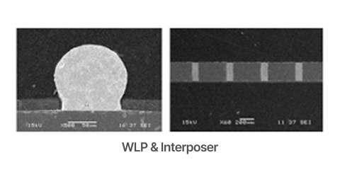
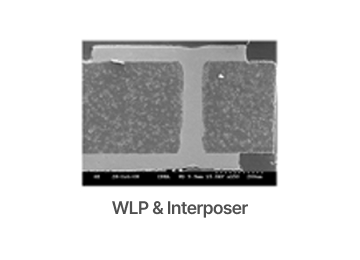
Enables the creation of cavity packages through TSV Wafer Level Packaging (WLP)
Facilitates the production of interposers that integrate large-scale PCBs with fine-scale chip devices using TSV
TSV interposer for 3D interconnection
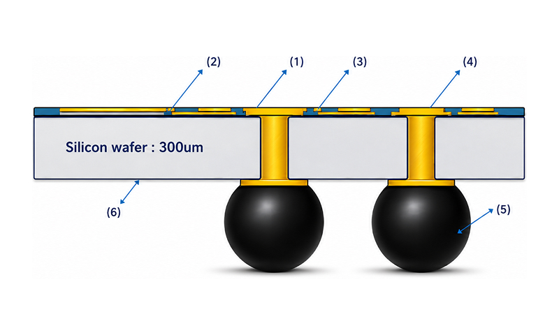
| NO | SPECIFICATION | PROCESS |
|---|---|---|
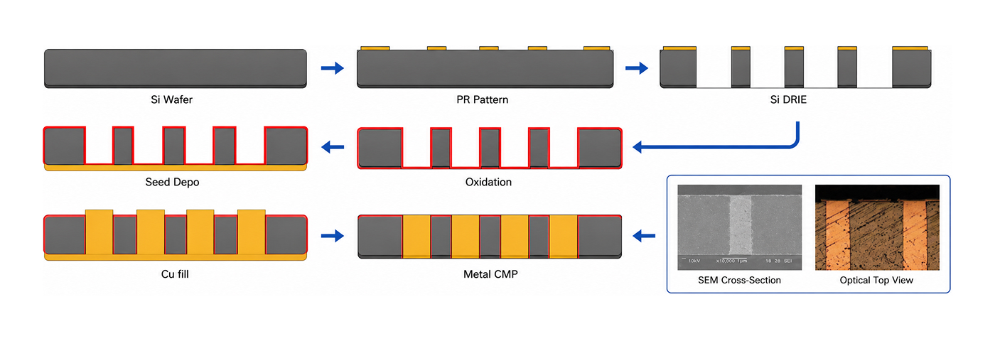
| 01 | Seed metal : Ti/Cu, Cr/Cu.... | Sputtering process E-Beam evaporation |
| 02 | RDL process : Cu, Au, Al.... | Sputter, E-Beam, Electroplating.. |
| 03 | Passivation layer PI, WPR, Su-8, SiO₂, SixNy.....Pat | Patterning, RIE, PE-CVD |
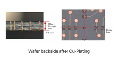
| 04 | Via filling : Cu | Electroplating |
| 05 | BGA or Bumping process | |
| 06 | SiO₂ 1um | Thermal oxidation |
Process flow