SOI Wafer

SOI Wafer (Silicon-on-Insulator)
An SOI (Silicon-on-Insulator) wafer consists of a thin silicon device layer separated from the silicon substrate
by a buried oxide (BOX) layer.
The BOX layer can serve as a sacrificial layer for releasing movable structures
in MEMS devices such as gyroscopes and accelerometers,
as well as an etch-stop or electrical isolation layer in various MEMS structures.
EPG provides SOI wafer fabrication based on its wafer bonding
and CMP (Chemical Mechanical Polishing) capabilities and dedicated process infrastructure.
Process flow
-
1
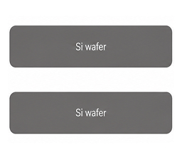
Wafer Inspection 및 Cleaning
-
2
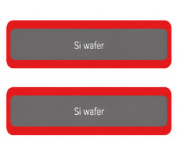
Thermal Oxidation / initial
-
3
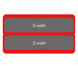
1100 ℃ anneal
-
4
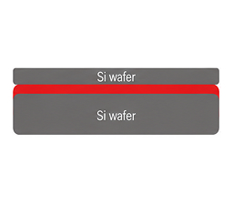
IR Inspection / CMP
SOI Structure
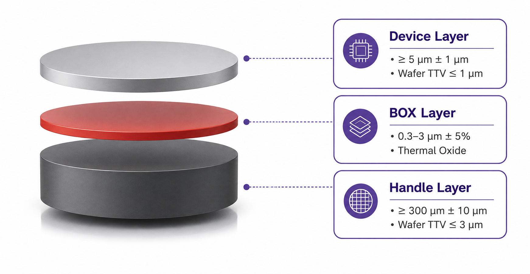
Standard Specifications
| 항목 | 사양 |
|---|---|
| Item Specification |
|
| Diameter |
4", 6", 8" |
| Conductivity Type |
P - type or N - type |
| Crystal Orientation |
<100>, <111>, <110> |
| Resistivity Range |
0.001 ~ 10000 Ω · cm |
| Surface Finish |
Single or Double Side Polished |
| Lead Time |
2 ~ 4 Weeks |