Cu post bump

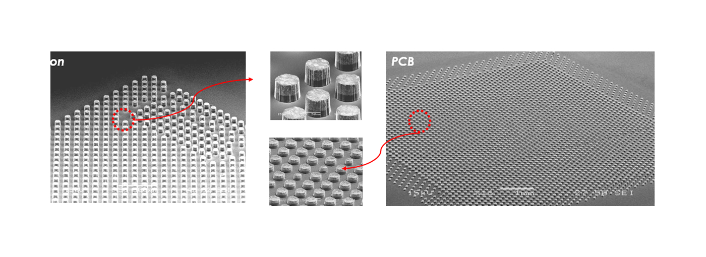
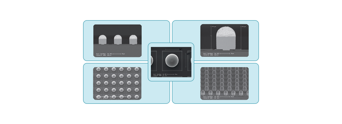
CPBT® (Copper Post Bump TEG)
TEG(Test Element Group) Wafer
A TEG (Test Element Group) wafer is used to evaluate the electrical characteristics
and performance of semiconductor devices and packaging structures.
EPG provides customized TEG wafers based on customer designs for various applications,
including package development, assembly process development, inspection equipment development, and material evaluation.
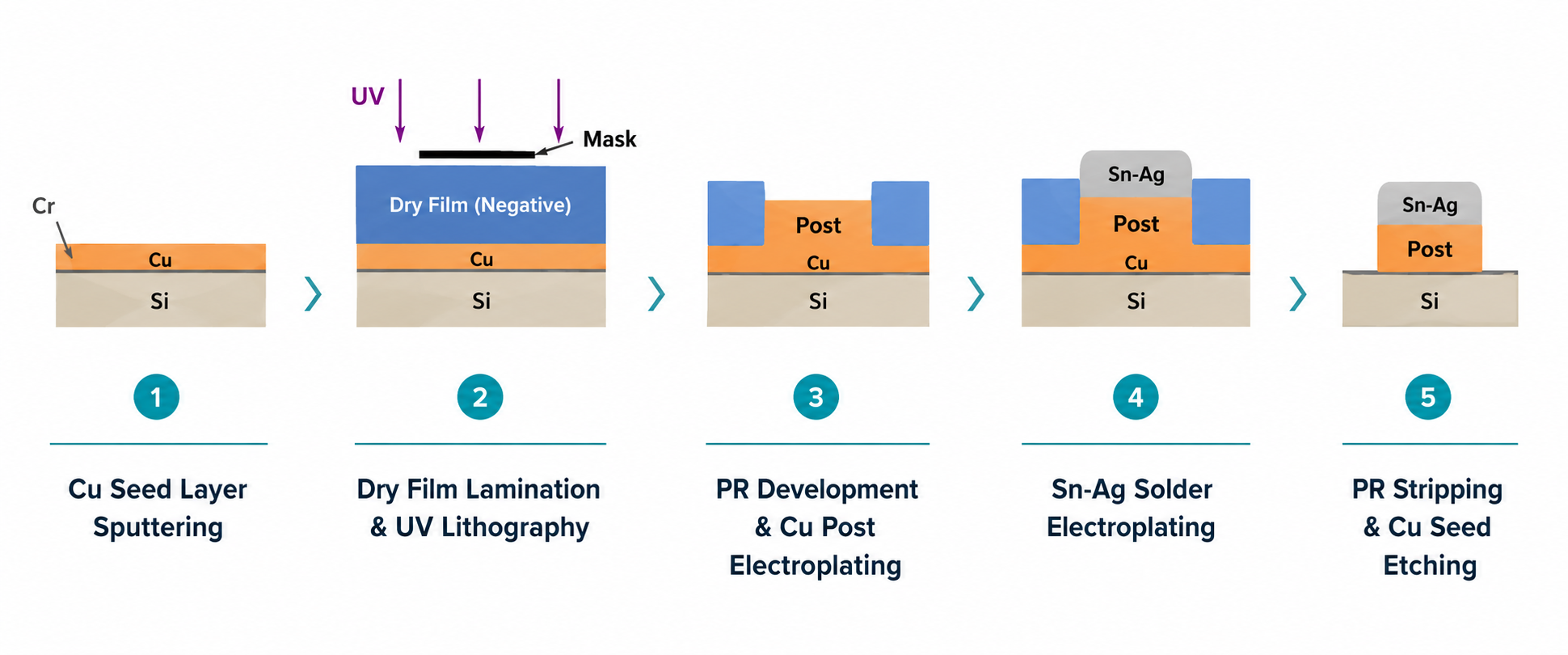
For fine-pitch applications, EPG's CPBT technology forms Sn-Ag solder bumps on electroplated Cu posts.
RDL (Redistribution Layer) structures can also be incorporated for electrical evaluation.