SOI Wafer

SOI Wafer (Si On Insulator)
An SOI (Silicon On Insulator) wafer features a SiO2 layer, known as the BOX (Buried Oxide) layer, in the middle of the wafer.
This SiO2 layer serves as a sacrificial layer to form the spring structure of gyroscopes and
accelerometers or as an etch stop layer and intermediate insulation layer for various MEMS structures,
allowing for diverse applications.
EPG possesses advanced bonding and CMP (Chemical Mechanical Polishing) process technologies, along with
the necessary infrastructure for the manufacturing of SOI wafers.
Process flow
-
1
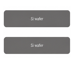
Wafer Inspection 및 Cleaning
-
2
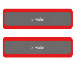
Thermal Oxidation / initial
-
3
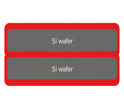
1100 ℃ anneal
-
4
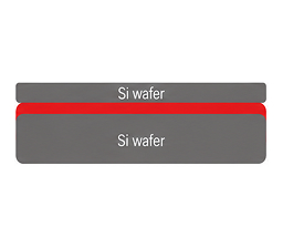
IR Inspection / CMP
SOI Structure
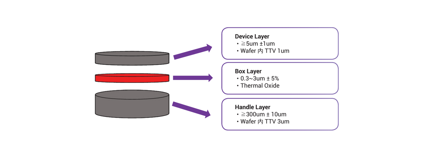
Standard Specifications
| 항목 | 사양 |
|---|---|
| Diameter | P - type or N - type |
| Conductivity Type | <100>, <111>, <110> |
| Resistivity Range | 0.001 ~ 10000 Ω |
| Surface finish | Single or Double Side Polished |
| Delivery | 2 ~ 4 Week |