TSV interposer

Advanced TSV Packaging Solutions
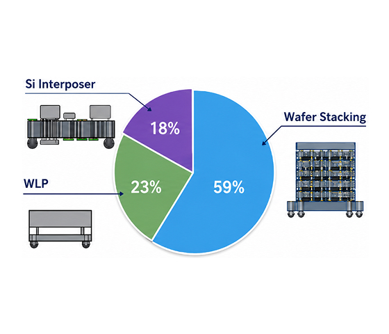
TSV (Through-Silicon Via) technology enables high-density vertical interconnections for advanced 3D semiconductor packaging.
It supports applications such as chip and wafer stacking,
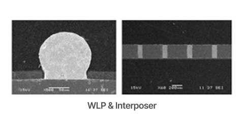
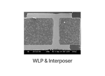
wafer-level packaging (WLP), and silicon interposers for high-density integration.
EPG provides TSV fabrication and related processes for the development of advanced packaging solutions.
TSV Interposer for 3D Integration
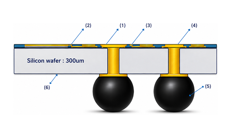
| NO | SPECIFICATION | PROCESS |
|---|---|---|
| 01 | Seed Metal: Ti/Cu, Cr/Cu, etc. |
Sputtering, E-Beam Evaporation |
| 02 | RDL Metal: Cu, Au, Al, etc. |
Sputtering, E-Beam Evaporation, Electroplating |
| 03 | Passivation Layer: PI, WPR, SU-8, SiO₂, SiNₓ, etc. |
Photolithography, RIE, PECVD |
| 04 | Via Filling: Cu |
Electroplating |
| 05 | BGA / Bump Formation |
Electroplating |
| 06 | Thermal SiO₂: 1~2 µm |
Thermal Oxidation |
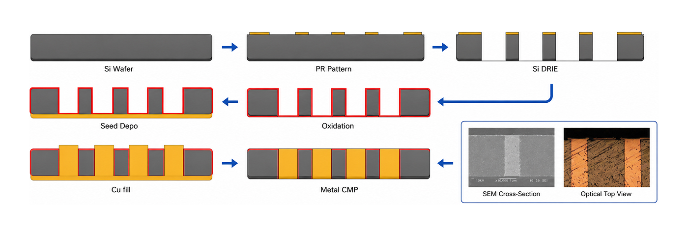
Process flow